Argomenti trattati
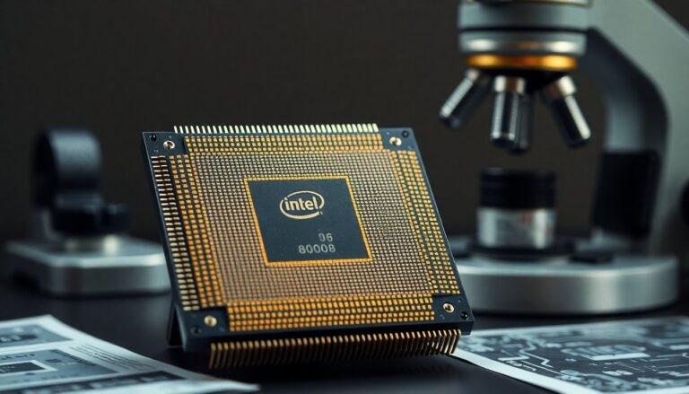
The evolution of computer technology has seen significant milestones, notably with the introduction of the Intel 8008 processor. This early 8-bit chip, developed in the early 1970s, established the groundwork for modern computing. Recent advancements in microscopy allow enthusiasts to showcase detailed images of this historic chip, highlighting its intricate structure and design.
Recently, a CPU collector known as CPU Duke shared a series of high-resolution images that explore the architecture of the Intel 8008. By meticulously capturing and stitching together 216 individual micrographs, CPU Duke has created an impressive visual representation of the chip, enabling an appreciation of its design in unprecedented detail.
The facts
The Intel 8008 made its debut in April 1972, crafted by the same team that developed the i4004 processor. This microprocessor was fabricated using a 10-micron PMOS process in Barbados, where Intel operated an assembly facility until 1986. The significance of the 8008 is profound, marking Intel’s first venture into 8-bit architecture and a pivotal shift in computing capabilities.
Collaboration with computer museums
The chip examined by CPU Duke was provided by the ENTER Technikwelt, a computer museum in Solothurn, Switzerland. The museum’s request for detailed imagery of this historic CPU underscores the growing interest in preserving and understanding the roots of computing technology. This collaboration has fostered appreciation for the 8008 and allowed enthusiasts to engage in the art of CPU microscopy.
The imaging process
Creating a detailed die shot of the Intel 8008 required a careful and intricate process. CPU Duke performed decapping, which involves removing the protective casing of the CPU to expose its silicon die. This process entailed heating the chip to approximately 600 degrees Celsius and delicately prying open the casing with a screwdriver blade, ensuring the internal structure remained intact for imaging.
Once the die was revealed, the initial imaging step involved capturing a series of macrographs to provide an overview of the chip’s features. Following this, CPU Duke used a Wild/Leica stereomicroscope equipped with a phototube to capture more granular details. The final product, a stitched micrograph, required aligning 216 separate images to showcase the complexity of the 8008’s architecture.
Understanding the architecture
The design of the Intel 8008 reveals noteworthy features at a glance. The 18-pin bond pad connectors, which serve as the interface between the chip and its socket, are distinctly visible. Additionally, markings such as ‘Intel 1971’, ‘8008’, and ‘HF’ pay tribute to the chip’s legacy and its design team, especially Hal Freeny, a key figure in the development of this groundbreaking microprocessor.
The 10-micron PMOS structure of the 8008 is significant, allowing for effective use of light microscopy techniques. As CPU Duke noted, the p-channel MOS structure can be differentiated under the metal surface, with semiconducting polysilicon appearing dark green and non-conducting areas showing a bright green hue in the microscopy images.
While the final stitched image of the Intel 8008 may lack color-coding overlays for clarity, the work of computer historian Ken Shirriff provides valuable insights into the architecture of this historic chip. His analysis enables enthusiasts and researchers to correlate the detailed images with specific components such as the ALU, registers, and data bus. Collaborative efforts ensure that the legacy of the Intel 8008 continues to inspire and educate future generations of technologists.
Advancements in microscopy and imaging technology promise deeper insights into the microprocessors that have shaped the digital landscape. The journey of the Intel 8008 serves as a testament to the lasting impact of early innovations on the evolution of computing.

