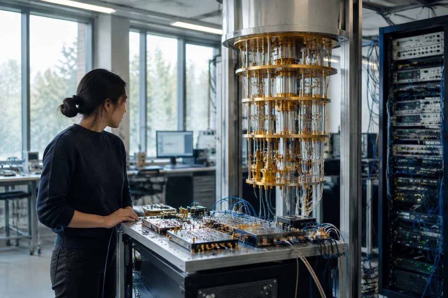
Quantum computing latency: clear definition and scope
Latency in quantum computing means the elapsed time between issuing an instruction and obtaining its effect on the quantum state or its classical outcome. Latency manifests at many points in a quantum system: within the physical qubits themselves, in the control electronics that generate pulses and readouts, and across the interconnects that link modules or extend systems geographically. Understanding latency requires separating its components, because each component constrains different aspects of throughput, fidelity and the ability to run real-world workloads.
Latency matters because quantum processors are limited by coherence times, gate durations and classical feedback loops. Excess latency reduces effective circuit depth, forces conservative scheduling, and can increase logical error rates after error correction. This article explains the principal latency sources, compares architectural choices such as surface code error correction, photonic links, and cryo-CMOS controllers, and evaluates their trade-offs for throughput, fidelity and practical workloads. The structure covers qubit-level physics, controls and interconnects, error-correction implications, workload mapping, and operational exceptions.
Qubits: intrinsic latency sources and their impact
At the device level, latency arises from gate durations and measurement time. Superconducting qubits typically use microwave pulses with gate times set by coupling strengths and anharmonicity, while spin qubits use exchange or magnetic resonance operations with different durations. Measurement latency depends on the readout mechanism and required signal-to-noise ratio: dispersive readout often involves integrating a microwave signal and digitizing it, which imposes an integration window. These physical limits interact with coherence time: longer gates or slow readout consume coherence budget and reduce usable algorithm depth. The result is a trade-off between fast gates that may be lower fidelity and slower gates that preserve fidelity but limit throughput.
Control electronics: from room temperature DACs to cryo-CMOS
Control systems create pulses, perform real-time demodulation, and implement feedback. Traditional stacks place arbitrary waveform generators and digitizers at room temperature, sending signals through attenuated cabling to the cryogenic stage. Latency appears as propagation delay and conversion or buffering time in digital-to-analog converters and field-programmable gate arrays. Moving control closer to qubits with cryo-CMOS reduces cable length and propagation delay and can enable faster feedback loops. However, integrating active electronics in cryogenic environments introduces thermal load and design complexity. Choosing cryo-CMOS improves real-time classical processing latency and can increase effective throughput, but requires careful trade-offs between heat dissipation, noise injection and manufacturability.
Interconnects and links: electrical, microwave and photonic trade-offs
Connecting qubits within a cryostat or between modules introduces latency from propagation and protocol overhead. Electrical and microwave links are low-latency over short distances but scale poorly across racks or buildings. Photonic links enable long-distance quantum connections with potentially lower latency per unit distance for fiber-optic transmission, and they simplify multiplexing. Photonic approaches typically add conversion latency (transducing microwave qubits to optical carriers) and probabilistic entanglement steps that impose handshake delays. For modular architectures, interconnect latency directly limits parallelism and the ability to run distributed error correction cycles within coherence windows. Design choices therefore balance raw propagation delay, conversion overhead and multiplexing efficiency.
Error correction and architecture: surface code versus alternatives
Error-correcting codes impose structured cycles of syndrome extraction and classical decoding. The surface code is widely used in architectural analysis because its syndrome cycles map to repeated local operations and fast classical decoding requirements. Surface-code cycles must complete syndrome measurement and apply corrections before logical errors grow; therefore, latency in measurement, classical processing and control feedback directly affects logical fidelity. Alternate codes with lower-weight checks or bosonic encodings change the cadence of correction and can relax some latency constraints at the cost of different overheads. Ultimately, error correction converts physical-latency budgets into logical time budgets: shorter physical latency reduces the required hardware redundancy for a target logical throughput.
Mapping real-world workloads: throughput, fidelity and scheduling
Workloads such as quantum chemistry simulations or optimization algorithms differ in depth, parallelism and tolerance for noise. High-depth circuits demand low-latency control and fast error correction to preserve logical fidelity across many layers of gates. Workloads with abundant parallelism benefit from architectures that minimize interconnect contention and support low-latency concurrent control channels. Scheduler design must account for measurement latency, classical processing delays and any inter-module handshake. For throughput, the key metrics are successful logical operations per second and effective circuit depth under error correction; both are sensitive to latency at qubit, control and interconnect layers.
Practical insights and notable exceptions
Some systems tolerate higher latency because their qubits have very long coherence times or because target algorithms are shallow and error-tolerant. Photonic networks excel for distributed entanglement but add conversion complexity that may not suit low-latency local operations. Cryo-CMOS reduces control latency but shifts engineering difficulty into cryogenic integration and thermal design. Surface-code architectures demand low-latency classical decoding, yet alternative codes may reduce decoding urgency but increase other resource costs. Choosing an architecture requires matching the latency profile to the workload’s depth and parallelism while accounting for practical engineering limits.
Practical indications for designers and users
Designers should measure and budget latency at each layer: gate and readout times for the qubits, conversion and processing times for control electronics, and handshake or transduction times for interconnects. Optimize the slowest stage first to improve end-to-end throughput. When selecting error correction, quantify how syndrome cycle latency translates into logical error rates for intended workloads. For practitioners planning experiments or applications, prioritize architectures where control latency aligns with algorithm demands: shallow, high-parallelism tasks tolerate interconnect-induced delays better than deep, sequential algorithms. Consider prototyping with mixed approaches, for example cryo-CMOS for critical feedback loops alongside photonic links for modular scaling.
Adopting a metric that combines fidelity and latency, such as successful logical operations per second at a target logical error rate, allows apples-to-apples comparison across architectures and informs procurement and design choices; practicing teams can run representative benchmarks to convert architectural latency trade-offs into concrete capacity and cost estimates.